ELEC 4706 -- Digital SERDES with Clock and Data Recovery
Author: Colin Byrne (101224212)
Institution: Carleton University
Date: December 4, 2025
1. Introduction
This laboratory focused on the design, implementation, and hardware verification of a complete SERDES system incorporating a pseudo-random bit sequence (PRBS) generator, frame-recovery logic, a clock-and-data-recovery (CDR) loop, and a real-time error-counting subsystem. The objective was to build a functional digital CDR capable of extracting timing information from an incoming data stream and reproducing a correctly aligned recovered clock and recovered data signal.
The system was first validated through functional simulation to confirm correctness of PRBS alignment, phase detection, and loop-filter behavior. The design was then synthesized and deployed on the DE1-SoC board, where oscilloscope measurements were used to assess timing, lock behavior, and the integrity of the recovered bitstream.
2. Process
System Integration and Top-Level Design
The first step involved creating the SERDES_TOP module, which interfaced the internal CDR logic with the DE1-SoC I/O. GPIO pins were configured as bidirectional signals to allow an external signal generator to drive the transmit clock while routing the input data, recovered data, and recovered clock to an oscilloscope. Reset signals were mapped to on-board pushbuttons, and the seven-segment displays were used to present the 16-bit error counter output.
The SERDES module integrated the PRBS transmitter and CDR, frame recovery logic, receive-side PRBS generator, and the error counter. Retiming flip-flops were used to ensure alignment between recovered data and reference PRBS bits before comparison.
PRBS Generation and Frame Recovery
The PRBS generator implemented the polynomial x^10 + x^7 + 1 and reset to an initial state of all ones. Since this PRBS sequence produces ten consecutive logic ones once every 1023 bits, the frame recovery block used a 10-bit shift register followed by an and_reduce() operation to detect alignment.
Upon detection, the receive-side PRBS generator was reset, ensuring alignment between transmitted and recovered bitstreams. Additional retiming stages were included to correct minor timing offsets.
CDR Implementation
The CDR architecture consisted of an 8-phase phase generator, a phase rotator controlled by increment and decrement signals, a bang-bang phase detector, a digital loop filter, and a clock divider. Together, these blocks generated a recovered sampling clock and synchronized recovered data.
Error Counter and Display
Recovered data and the receive-side PRBS reference were XORed and passed through a retiming flip-flop before being counted. A 16-bit error counter accumulated bit mismatches, and the count was displayed in hexadecimal on the seven-segment displays.
Functional Simulation
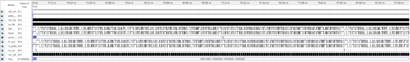
Functional simulation was performed using a PRBS clock of 12.5 MHz and a reference clock of 100 MHz. These values preserved timing relationships while reducing simulation time. The simulation confirmed successful frame detection, PRBS alignment, and zero error accumulation after lock.
On-Board Hardware Verification
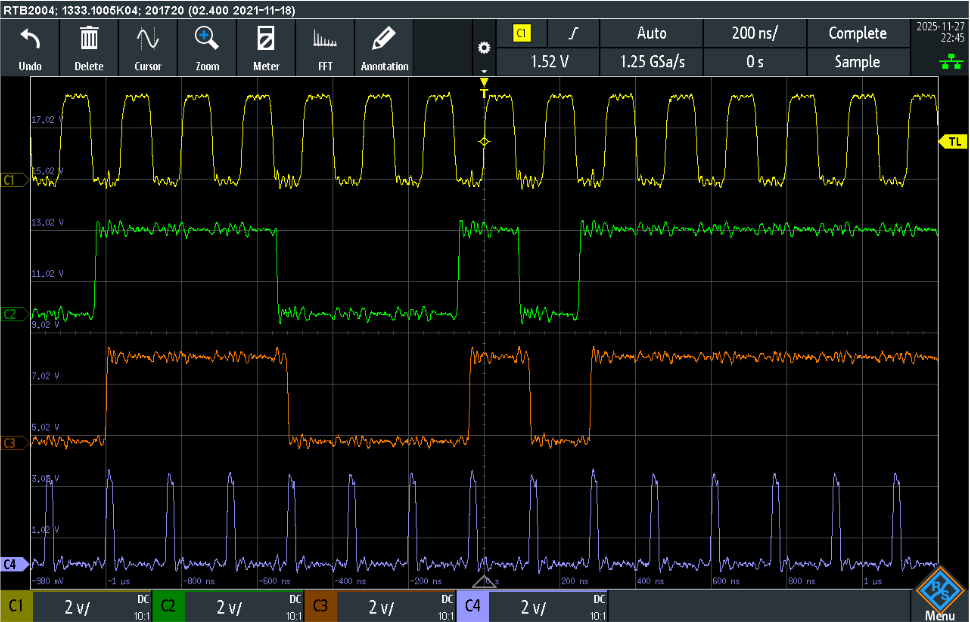
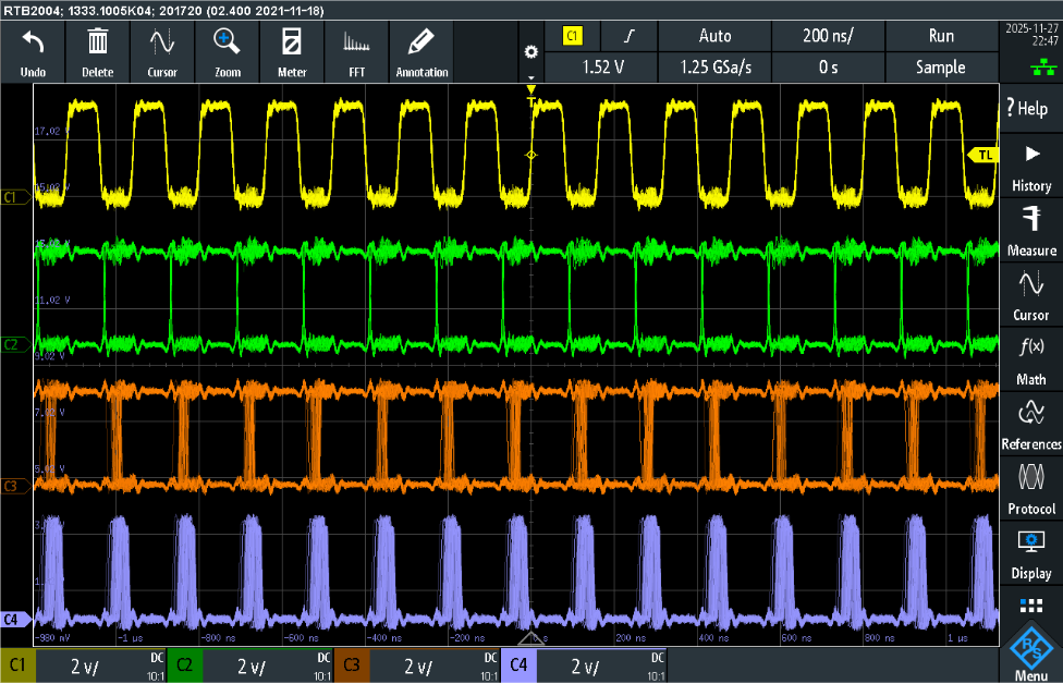
After simulation, the design was synthesized and programmed onto the DE1-SoC board. A 6.25 MHz clock was applied to the transmitter, while the on-board 50 MHz clock drove the CDR. Oscilloscope measurements were used to observe input data, recovered data, recovered clock, and eye diagrams.
3. Results
Simulation Results
Hardware Results
4. Conclusion
The implemented SERDES and CDR system successfully met all design objectives. Functional simulation confirmed correct PRBS alignment, stable CDR operation, and error-free data recovery. Hardware verification further demonstrated reliable clock recovery, stable phase alignment, and accurate data sampling. Overall, the design represents a complete and functional digital CDR implemented on the DE1-SoC platform.
5. Appendix: VHDL Source Code
SERDES TOP
-- SERDES_TOP.vhd
library IEEE;
use IEEE.STD_LOGIC_1164.ALL;

entity SERDES_TOP is
	port(
	KEY : in std_logic_vector(1 downto 0);
	CLOCK_50 : in std_logic;
	GPIO_O : inout std_logic_vector(3 downto 0);
   -- 7-segment displays
   HEX3 : out std_logic_vector(6 downto 0);
   HEX2 : out std_logic_vector(6 downto 0);
   HEX1 : out std_logic_vector(6 downto 0);
   HEX0 : out std_logic_vector(6 downto 0)
	);
end SERDES_TOP;

architecture Structural of SERDES_TOP is
	--SERDES
	component SERDES is
		Port(
			tx_clk : in STD_LOGIC;
			ref_clk : in STD_LOGIC;
			prbs_rst : in STD_LOGIC;
			cdr_rst : in STD_LOGIC;
			Din : out STD_LOGIC;
			Dout : out STD_LOGIC;
			rec_clk : out STD_LOGIC;
			HEX3 : out std_logic_vector(6 downto 0);
			HEX2 : out std_logic_vector(6 downto 0);
			HEX1 : out std_logic_vector(6 downto 0);
			HEX0 : out std_logic_vector(6 downto 0)
		);
	end component;

	begin

	U_SERDES : SERDES
		Port map(
			tx_clk => GPIO_O(0),
			ref_clk => CLOCK_50,
			prbs_rst => KEY(1),
			cdr_rst => KEY(0),
			Din => GPIO_O(1),
			Dout => GPIO_O(2),
			rec_clk => GPIO_O(3),
			HEX3 => HEX3,
			HEX2 => HEX2,
			HEX1 => HEX1,
			HEX0 => HEX0
		);

	end Structural;
SERDES
-- SERDES.vhd
library IEEE;
use IEEE.STD_LOGIC_1164.ALL;

entity SERDES is
	Port(
	tx_clk : in STD_LOGIC;
	ref_clk : in STD_LOGIC;
	prbs_rst : in STD_LOGIC;
	cdr_rst : in STD_LOGIC;
	rx_prbs : out std_LOGIC;
	fr_out : out std_LOGIC;
	rx_rst: out std_LOGIC;
	Din : out STD_LOGIC;
	Dout : out STD_LOGIC;
	rec_clk : out STD_LOGIC;
	error_cnt : out STD_LOGIC_VECTOR(15 downto 0);
	HEX3 : out std_logic_vector(6 downto 0);
	HEX2 : out std_logic_vector(6 downto 0);
	HEX1 : out std_logic_vector(6 downto 0);
	HEX0 : out std_logic_vector(6 downto 0)
	);
end SERDES;

architecture Structural of SERDES is
	-- Internal Singals
	signal Dout_signal, rec_clk_sig : std_LOGIC;
	signal Rx_rst_sig : std_LOGIC;
	signal FR_xor_in, RX_xor_in, xor_out, xor_out_good : std_logic;
	signal FR_Q, RX_out : std_LOGIC;
	--Components
	component Top_Test is
		port(
		tx_clk : in STD_LOGIC;
		ref_clk : in STD_LOGIC;
		prbs_rst : in STD_LOGIC;
		cdr_rst : in STD_LOGIC;
		Dout : out STD_LOGIC;
		rec_clk : out STD_LOGIC;
		Din : out STD_LOGIC
	);
	end component;

	component PRBS_Generator is
		port (
        clk     : in  std_logic;
        reset   : in  std_logic;
        bit_out : out std_logic;
        q_out   : out std_logic_vector(9 downto 0)
		);
	end component;

	component colin_frame_recovery is
		Port(
			Dout : in STD_LOGIC;
			clk : in STD_LOGIC;
			rst : in STD_LOGIC;
			Q : out STD_LOGIC;
			Rx_rst : out STD_LOGIC
		);
	end component;

	component colin_error_counter is
		Port(
			xor_in : in std_logic;
			clk : in std_logic;
			rst : in std_logic;
			count : out std_logic_vector(15 downto 0);
			HEX3 : out std_logic_vector(6 downto 0);
			HEX2 : out std_logic_vector(6 downto 0);
			HEX1 : out std_logic_vector(6 downto 0);
			HEX0 : out std_logic_vector(6 downto 0)
		);
	end component;

	component DFF_Custom is
		Port (
			clk   : in  STD_LOGIC;
			reset : in  STD_LOGIC;
			D     : in  STD_LOGIC;
			reset_value : in STD_LOGIC;
			Q     : out STD_LOGIC
		);
	end component;

	begin

	U_TopTest : Top_Test
		port map(
			tx_clk => tx_clk,
			ref_clk => ref_clk,
			prbs_rst => prbs_rst,
			cdr_rst => cdr_rst,
			Dout => Dout_signal,
			rec_clk => rec_clk_sig,
			Din => Din
		);

	U_FR : colin_frame_recovery
		port map(
			Dout => Dout_signal,
			clk => rec_clk_sig,
			rst => cdr_rst,
			Q =>	FR_Q,
			Rx_rst => Rx_rst_sig
		);

	U_RXPRBS : PRBS_Generator
		port map(
			clk => rec_clk_sig,
			reset => Rx_rst_sig,
			bit_out => RX_out
		);

	FR_Latch : DFF_Custom
		port map(
			D => RX_out,
			clk => rec_clk_sig,
			reset => not(cdr_rst),
			reset_value => '0',
			Q => RX_xor_in
		);


	FRQ_FF : DFF_Custom
		port map(
			D => FR_Q,
			clk => rec_clk_sig,
			reset => not(cdr_rst),
			reset_value => '0',
			Q => FR_xor_in
		);

	xor_out <= FR_xor_in xor RX_xor_in;

	RX_FF : DFF_Custom
		port map(
			D => xor_out,
			clk => rec_clk_sig,
			reset => not(cdr_rst),
			reset_value => '0',
			Q => xor_out_good
		);


	U_EC : colin_error_counter
		port map(
			xor_in => xor_out_good,
			clk => rec_clk_sig,
			rst => cdr_rst,
			count => error_cnt,
			HEX3 => HEX3,
			HEX2 => HEX2,
			HEX1 => HEX1,
			HEX0 => HEX0
		);

	Dout <= Dout_signal;
	rec_clk <= rec_clk_sig;
	rx_prbs <= RX_xor_in;
	FR_out <= FR_xor_in;
	rx_rst <= rx_rst_sig;


end Structural;
Frame Recover
-- colin_frame_recovery.vhd
library IEEE;
use IEEE.STD_LOGIC_1164.ALL;
use IEEE.STD_LOGIC_MISC.ALL;

entity colin_frame_recovery is
	Port(
		Dout : in STD_LOGIC;
		clk : in STD_LOGIC;
		rst : in STD_LOGIC;
		Q : out STD_LOGIC;
		parallel_out : out STD_LOGIC_VECTOR(9 downto 0);
		Rx_rst : out STD_LOGIC;
		d_latch : out std_LOGIC
	);
end colin_frame_recovery;

architecture Structural of colin_frame_recovery is
	--Internal signals
	signal serial_out, d_latch_sig : STD_LOGIC;
	signal parallel_out_sig : STD_LOGIC_VECTOR(9 downto 0);

	component colin_shift_reg is
		port(
			clk    : in  std_logic;
			rst    : in  std_logic;  -- synchronous reset
			sin    : in  std_logic;  -- serial input
			sout   : out std_logic;  -- serial output
			q      : out std_logic_vector(9 downto 0)  -- internal contents
		);
	end component;

	 component colin_latch is
		port(
			D : in STD_LOGIC;
			en : in STD_LOGIC;
			rst : in STD_LOGIC;
			Q : out STD_LOGIC
		);
	end component;

	component DFF_Custom is
		Port (
			clk   : in  STD_LOGIC;
			reset : in  STD_LOGIC;
			D     : in  STD_LOGIC;
			reset_value : in STD_LOGIC;
			Q     : out STD_LOGIC
		);
	end component;

	begin

	FR_Shift_Reg : colin_shift_reg
		port map(
			clk => clk,
			rst => not(rst),
			sin => Dout,
			sout => serial_out,
			Q => parallel_out_sig
		);

	d_latch_sig <= and_reduce(parallel_out_sig);

	FR_Latch : DFF_Custom
		port map(
			D => d_latch_sig,
			clk => clk,
			reset => not(rst),
			reset_value => '0',
			Q => RX_rst
		);

	FR_DFF : DFF_Custom
		port map(
			clk => clk,
			reset => not(rst),
			D => serial_out,
			reset_value => '0',
			Q => Q
		);

		d_latch <= d_latch_sig;
		parallel_out <= parallel_out_sig;

end Structural;
Shift Register
-- colin_shift_reg.vhd
library IEEE;
use IEEE.STD_LOGIC_1164.ALL;

entity colin_shift_reg is
    port (
        clk    : in  std_logic;
        rst    : in  std_logic;  -- synchronous reset
        sin    : in  std_logic;  -- serial input
        sout   : out std_logic;  -- serial output
        Q      : out std_logic_vector(9 downto 0)  -- internal contents
    );
end colin_shift_reg;

architecture Structural of colin_shift_reg is
		signal qo : std_logic_vector(9 downto 0);
		signal d : std_logic_vector(9 downto 0);
		signal reset_bits : std_logic_vector(9 downto 0);
begin

    --------------------------------------------------------------------
    -- Next-state logic
    --------------------------------------------------------------------
    d(9) <= qo(8);
    d(8) <= qo(7);
    d(7) <= qo(6);
    d(6) <= qo(5);
    d(5) <= qo(4);
    d(4) <= qo(3);
    d(3) <= qo(2);
    d(2) <= qo(1);
    d(1) <= qo(0);
    d(0) <= sin;

    reset_bits(9) <= '0';
    reset_bits(8) <= '0';
    reset_bits(7) <= '0';
    reset_bits(6) <= '0';
    reset_bits(5) <= '0';
    reset_bits(4) <= '0';
    reset_bits(3) <= '0';
    reset_bits(2) <= '0';
    reset_bits(1) <= '0';
    reset_bits(0) <= '0';

    gen_dffs : for i in 0 to 9 generate
    begin
        DFF_inst : entity work.DFF_Custom
            port map (
                clk         => not(clk),
                reset       => rst,
                D           => d(i),
                reset_value => reset_bits(i),  -- per-bit reset value
                Q           => qo(i)
            );
    end generate;


    Q   <= qo;
    sout <= qo(9);


end Structural;
Error Counter
-- colin_error_counter.vhd
library IEEE;
use IEEE.std_logic_1164.all;
--Colin Byrne 101224212
entity colin_error_counter is
	Port(
		xor_in : in std_logic;
		clk : in std_logic;
		rst : in std_logic;
		count : out std_logic_vector(15 downto 0);
		HEX3 : out std_logic_vector(6 downto 0);
		HEX2 : out std_logic_vector(6 downto 0);
		HEX1 : out std_logic_vector(6 downto 0);
		HEX0 : out std_logic_vector(6 downto 0)
	);
end colin_error_counter;

architecture Structural of colin_error_counter is

	--Internal Signals
	signal count_signal : STD_LOGIC_VECTOR(15 downto 0);

	component colin_counter is
		Port(
			xor_in : in STD_LOGIC;
			clk : in STD_LOGIC;
			rst : in STD_LOGIC;
			count : out STD_LOGIC_VECTOR(15 downto 0)
		);
	end component;

	component seven_segment_decoder is
		Port(
			SW : in STD_LOGIC_VECTOR(3 downto 0);   -- 4-bit input from switches
			HEX0 : out STD_LOGIC_VECTOR(6 downto 0) -- 7-segment display output
		);
	end component;

begin

	counter16 : colin_counter
		port map(
			xor_in => xor_in,
			clk => clk,
			rst => rst,
			count => count_signal
		);

	sevenseg0 : seven_segment_decoder
		port map(
			SW => count_signal(3 downto 0),
			HEX0 => HEX0
		);

	sevenseg1 : seven_segment_decoder
		port map(
			SW => count_signal(7 downto 4),
			HEX0 => HEX1
		);

	sevenseg2 : seven_segment_decoder
		port map(
			SW => count_signal(11 downto 8),
			HEX0 => HEX2
		);

	sevenseg3 : seven_segment_decoder
		port map(
			SW => count_signal(15 downto 12),
			HEX0 => HEX3
		);

		count <= count_signal;

end Structural;
Seven Segment Decoder
-- seven_segment_decoder.vhd
library IEEE;
use IEEE.STD_LOGIC_1164.ALL;

entity seven_segment_decoder is
    Port (
        SW : in STD_LOGIC_VECTOR(3 downto 0);   -- 4-bit input from switches
        HEX0 : out STD_LOGIC_VECTOR(6 downto 0) -- 7-segment display output
    );
end seven_segment_decoder;


architecture Behavioral of seven_segment_decoder is
begin
    process(SW)
    begin
        case SW is
            when "0000" => HEX0 <= "1000000"; -- 0
            when "0001" => HEX0 <= "1111001"; -- 1
            when "0010" => HEX0 <= "0100100"; -- 2
            when "0011" => HEX0 <= "0110000"; -- 3
            when "0100" => HEX0 <= "0011001"; -- 4
            when "0101" => HEX0 <= "0010010"; -- 5
            when "0110" => HEX0 <= "0000010"; -- 6
            when "0111" => HEX0 <= "1111000"; -- 7
            when "1000" => HEX0 <= "0000000"; -- 8
            when "1001" => HEX0 <= "0010000"; -- 9
            when "1010" => HEX0 <= "0001000"; -- A
            when "1011" => HEX0 <= "0000011"; -- b
            when "1100" => HEX0 <= "1000110"; -- C
            when "1101" => HEX0 <= "0100001"; -- d
            when "1110" => HEX0 <= "0000110"; -- E
            when "1111" => HEX0 <= "0001110"; -- F
            when others => HEX0 <= "1111111"; -- All segments off (default)
        end case;
    end process;
end Behavioral;
DFF
-- DFF_Custom.vhd
library IEEE;
use IEEE.STD_LOGIC_1164.ALL;

entity DFF_Custom is
    Port (
        clk   : in  STD_LOGIC;
        reset : in  STD_LOGIC;
        D     : in  STD_LOGIC;
		  reset_value : in STD_LOGIC;
        Q     : out STD_LOGIC
    );
end DFF_Custom;

architecture Behavioral of DFF_Custom is
begin
    process (clk, reset)
    begin
			if reset = '1' then
				Q <= reset_value;
        elsif rising_edge(clk) then
            Q <= D; -- Latch D to Q on rising clock edge
        end if;
    end process;
end Behavioral;
PRBS Generator
-- PRBS_Generator.vhd
library ieee;
use ieee.std_logic_1164.all;
use ieee.std_logic_misc.all;

entity PRBS_Generator is
    port (
        clk     : in  std_logic;
        reset   : in  std_logic;
        bit_out : out std_logic;
        q_out   : out std_logic_vector(9 downto 0);
		  all_one : out std_logic
    );
end entity PRBS_Generator;

architecture Structural of PRBS_Generator is
    signal q : std_logic_vector(9 downto 0);
    signal d : std_logic_vector(9 downto 0);
    signal feedback_bit : std_logic;
    signal reset_bits : std_logic_vector(9 downto 0);
begin

    feedback_bit <= q(9) xor q(6);

    d(9) <= q(8);
    d(8) <= q(7);
    d(7) <= q(6);
    d(6) <= q(5);
    d(5) <= q(4);
    d(4) <= q(3);
    d(3) <= q(2);
    d(2) <= q(1);
    d(1) <= q(0);
    d(0) <= feedback_bit;

    reset_bits(9) <= '1';
    reset_bits(8) <= '1';
    reset_bits(7) <= '1';
    reset_bits(6) <= '1';
    reset_bits(5) <= '1';
    reset_bits(4) <= '1';
    reset_bits(3) <= '1';
    reset_bits(2) <= '1';
    reset_bits(1) <= '1';
    reset_bits(0) <= '1';

    gen_dffs : for i in 0 to 9 generate
    begin
        DFF_inst : entity work.DFF_Custom
            port map (
                clk         => not(clk),
                reset       => reset,
                D           => d(i),
                reset_value => reset_bits(i),  -- per-bit reset value
                Q           => q(i)
            );
    end generate;

    q_out   <= q;
    bit_out <= q(9);
	 all_one <= and_reduce(q);

end architecture Structural;
CDR
-- CDR.vhd
library IEEE;
use IEEE.STD_LOGIC_1164.ALL;

entity CDR is
    Port (
        Din           : in  STD_LOGIC;
        ref_clk       : in  STD_LOGIC;
        cdr_rst       : in  STD_LOGIC;
        Dout          : out STD_LOGIC;
        rec_clk       : out STD_LOGIC;
        Clk_early_out : out STD_LOGIC;
        Clk_edge_out  : out STD_LOGIC;
        Clk_late_out  : out STD_LOGIC;
        Up            : out STD_LOGIC;
        Down          : out STD_LOGIC;
        div_clk       : out STD_LOGIC;
        P0            : out STD_LOGIC;
        P1            : out STD_LOGIC;
        P2            : out STD_LOGIC;
        P3            : out STD_LOGIC;
        P4            : out STD_LOGIC;
        P5            : out STD_LOGIC;
        P6            : out STD_LOGIC;
        P7            : out STD_LOGIC;
        Out_P         : out STD_LOGIC;
        Out_N         : out STD_LOGIC;
        counter_out   : out STD_LOGIC_VECTOR(2 downto 0)
    );
end CDR;

architecture Structural of CDR is

    -- Internal Signals
    signal Clk_early_sig, Clk_edge_sig, Clk_late_sig : STD_LOGIC;
    signal DFF_Clk_late_sig, PR_clk_sig : STD_LOGIC;
    signal div_clk_sig : STD_LOGIC;
    signal P0_sig, P1_sig, P2_sig, P3_sig : STD_LOGIC;
    signal P4_sig, P5_sig, P6_sig, P7_sig : STD_LOGIC;
    signal up_sig, down_sig : STD_LOGIC;
    signal out_p_sig, out_n_sig : STD_LOGIC;
    signal rec_clk_sig : STD_LOGIC;

    -- Component Declarations
    component Phase_Generator is
        Port (
            clk : in STD_LOGIC;
            rst : in STD_LOGIC;
            P0  : out STD_LOGIC;
            P1  : out STD_LOGIC;
            P2  : out STD_LOGIC;
            P3  : out STD_LOGIC;
            P4  : out STD_LOGIC;
            P5  : out STD_LOGIC;
            P6  : out STD_LOGIC;
            P7  : out STD_LOGIC
        );
    end component;

    component Clock_Divider is
        Port (
            clk     : in STD_LOGIC;
            rst     : in STD_LOGIC;
            clk_div : out STD_LOGIC
        );
    end component;

    component Phase_Rotator is
        Port (
            clk_div     : in  STD_LOGIC;
            rst         : in  STD_LOGIC;
            INC         : in  STD_LOGIC;
            DEC         : in  STD_LOGIC;
            P0          : in  STD_LOGIC;
            P1          : in  STD_LOGIC;
            P2          : in  STD_LOGIC;
            P3          : in  STD_LOGIC;
            P4          : in  STD_LOGIC;
            P5          : in  STD_LOGIC;
            P6          : in  STD_LOGIC;
            P7          : in  STD_LOGIC;
            CLK_early   : out STD_LOGIC;
            CLK_edge    : out STD_LOGIC;
            CLK_late    : out STD_LOGIC;
            counter_out : out STD_LOGIC_VECTOR(2 downto 0)
        );
    end component;

    component DFF_Custom is
        Port (
            clk          : in  STD_LOGIC;
            reset        : in  STD_LOGIC;
            D            : in  STD_LOGIC;
            reset_value  : in  STD_LOGIC;
            Q            : out STD_LOGIC
        );
    end component;

    component BBPD is
        Port (
            Clk_early : in STD_LOGIC;
            Clk_edge  : in STD_LOGIC;
            Clk_late  : in STD_LOGIC;
            rst       : in STD_LOGIC;
            Data_in   : in STD_LOGIC;
            Up        : out STD_LOGIC;
            Down      : out STD_LOGIC
        );
    end component;

    component Digital_Filter is
        Port (
            clk    : in STD_LOGIC;
            rst    : in STD_LOGIC;
            In_P   : in STD_LOGIC;  -- Up signal from BBPD
            In_N   : in STD_LOGIC;  -- Down signal from BBPD
            Out_P  : out STD_LOGIC; -- INC to Phase Rotator
            Out_N  : out STD_LOGIC  -- DEC to Phase Rotator
        );
    end component;

begin

    -- Phase Generator (creates 8-phase clocks)
    U_Phase_Gen : Phase_Generator
        port map (
            clk => ref_clk,
            rst => cdr_rst,
            P0  => P0_sig,
            P1  => P1_sig,
            P2  => P2_sig,
            P3  => P3_sig,
            P4  => P4_sig,
            P5  => P5_sig,
            P6  => P6_sig,
            P7  => P7_sig
        );

    -- Phase Rotator (selects phases based on INC/DEC)
    U_Phase_Rot : Phase_Rotator
        port map (
            clk_div     => PR_clk_sig,
            rst         => cdr_rst,
            INC         => out_p_sig,
            DEC         => out_n_sig,
            P0          => P0_sig,
            P1          => P1_sig,
            P2          => P2_sig,
            P3          => P3_sig,
            P4          => P4_sig,
            P5          => P5_sig,
            P6          => P6_sig,
            P7          => P7_sig,
            CLK_early   => Clk_early_sig,
            CLK_edge    => Clk_edge_sig,
            CLK_late    => Clk_late_sig,
            counter_out => counter_out
        );

    -- DFF for Late Clock
    DFF_DIV : DFF_Custom
        port map (
            clk          => ref_clk,
            reset        => not(cdr_rst),
            D            => Clk_late_sig,
            reset_value  => '0',
            Q            => DFF_Clk_late_sig
        );

    -- Recovered Clock DFF
    DFF_REC : DFF_Custom
        port map (
            clk          => ref_clk,
            reset        => not(cdr_rst),
            D            => DFF_Clk_late_sig,
            reset_value  => '0',
            Q            => rec_clk_sig
        );

    -- Clock Divider (generates CLK/4)
    U_Clock_Div : Clock_Divider
        port map (
            clk     => DFF_Clk_late_sig,
            rst     => not(cdr_rst),
            clk_div => div_clk_sig
        );

    -- Phase Rotator Clock DFF
    DFF_POST_DIV : DFF_Custom
        port map (
            clk          => ref_clk,
            reset        => not(cdr_rst),
            D            => div_clk_sig,
            reset_value  => '0',
            Q            => PR_clk_sig
        );

    -- Phase Detector
    U_Phase_Det : BBPD
        port map (
            Clk_early => Clk_early_sig,
            Clk_edge  => Clk_edge_sig,
            Clk_late  => Clk_late_sig,
            rst       => cdr_rst,
            Data_in   => Din,
            Up        => up_sig,
            Down      => down_sig
        );

    -- Digital Filter
    U_Digital_Fil : Digital_Filter
        port map (
            clk    => DFF_Clk_late_sig,
            rst    => cdr_rst,
            In_P   => up_sig,
            In_N   => down_sig,
            Out_P  => out_p_sig,
            Out_N  => out_n_sig
        );

    -- DFF for Recovered Data
    DFF_REC_DATA : DFF_Custom
        port map (
            clk          => rec_clk_sig,
            reset        => not(cdr_rst),
            D            => Din,
            reset_value  => '0',
            Q            => Dout
        );

    -- Output assignments
    Clk_early_out <= Clk_early_sig;
    Clk_edge_out  <= Clk_edge_sig;
    Clk_late_out  <= Clk_late_sig;
    rec_clk       <= rec_clk_sig;
    Up            <= up_sig;
    Down          <= down_sig;
    div_clk       <= div_clk_sig;
    P0            <= P0_sig;
    P1            <= P1_sig;
    P2            <= P2_sig;
    P3            <= P3_sig;
    P4            <= P4_sig;
    P5            <= P5_sig;
    P6            <= P6_sig;
    P7            <= P7_sig;
    Out_P         <= out_p_sig;
    Out_N         <= out_n_sig;

end Structural;
Clock Divider
-- Clock_Divider.vhd
library IEEE;
use IEEE.STD_LOGIC_1164.ALL;
use IEEE.NUMERIC_STD.ALL;

entity Clock_Divider is
    Port (
        clk : in STD_LOGIC;
        rst : in STD_LOGIC;
        clk_div : out STD_LOGIC
    );
end Clock_Divider;

architecture Behavioral of Clock_Divider is
    signal clk_temp : STD_LOGIC := '0';
begin
    process(clk, rst)
	 variable div_counter : unsigned(1 downto 0) := "00";
    begin
        if rst = '1' then
            div_counter := "00";
            clk_temp <= '0';
        elsif falling_edge(clk) then
            if div_counter = "10" then
                div_counter := "00";
                clk_temp <= not clk_temp;
				end if;
            div_counter := div_counter + 1;
			end if;
    end process;

    clk_div <= clk_temp;
end Behavioral;
Digital Filter
-- Digital_Filter.vhd
library IEEE;
use IEEE.STD_LOGIC_1164.ALL;

entity Digital_Filter is
    Port (
        clk : in STD_LOGIC;
        rst : in STD_LOGIC;
        In_P : in STD_LOGIC;  -- Up signal from BBPD
        In_N : in STD_LOGIC;  -- Down signal from BBPD
        Out_P : out STD_LOGIC; -- INC to Phase Rotator
        Out_N : out STD_LOGIC  -- DEC to Phase Rotator
    );
end Digital_Filter;

architecture Behavioral of Digital_Filter is
    type shift_reg_type is array (0 to 3) of STD_LOGIC;
    signal up_shift_reg, down_shift_reg : shift_reg_type;
    signal up_or_out, down_or_out : STD_LOGIC;
begin

    -- Generate 4 DFFs for Up signal path
    UP_DFF_GEN: for i in 0 to 3 generate
        FIRST_UP: if i = 0 generate
            UP_DFF0: entity work.DFF_Custom
                port map (
                    clk => clk,
                    reset => not(rst),
                    D => In_P,
                    reset_value => '0',
                    Q => up_shift_reg(i)
                );
        end generate FIRST_UP;

        REST_UP: if i > 0 generate
            UP_DFF: entity work.DFF_Custom
                port map (
                    clk => clk,
                    reset => not(rst),
                    D => up_shift_reg(i-1),
                    reset_value => '0',
                    Q => up_shift_reg(i)
                );
        end generate REST_UP;
    end generate UP_DFF_GEN;

    -- Generate 4 DFFs for Down signal path
    DOWN_DFF_GEN: for i in 0 to 3 generate
        FIRST_DOWN: if i = 0 generate
            DOWN_DFF0: entity work.DFF_Custom
                port map (
                    clk => clk,
                    reset => not(rst),
                    D => In_N,
                    reset_value => '0',
                    Q => down_shift_reg(i)
                );
        end generate FIRST_DOWN;

        REST_DOWN: if i > 0 generate
            DOWN_DFF: entity work.DFF_Custom
                port map (
                    clk => clk,
                    reset => not(rst),
                    D => down_shift_reg(i-1),
                    reset_value => '0',
                    Q => down_shift_reg(i)
                );
        end generate REST_DOWN;
    end generate DOWN_DFF_GEN;

    -- OR gates (any of the four flip-flop outputs)
    up_or_out <= up_shift_reg(0) or up_shift_reg(1) or up_shift_reg(2) or up_shift_reg(3);
    down_or_out <= down_shift_reg(0) or down_shift_reg(1) or down_shift_reg(2) or down_shift_reg(3);

    -- AND gates with inverted inputs for mutual exclusion
    Out_P <= up_or_out and not down_or_out;
    Out_N <= down_or_out and not up_or_out;

end Behavioral;
BBPD
-- BBPD.vhd
library IEEE;
use IEEE.STD_LOGIC_1164.ALL;

entity BBPD is
    Port (
        Clk_early : in STD_LOGIC;
        Clk_edge  : in STD_LOGIC;
        Clk_late  : in STD_LOGIC;
        rst       : in STD_LOGIC;
        Data_in   : in STD_LOGIC;
        Up        : out STD_LOGIC;
        Down      : out STD_LOGIC
    );
end BBPD;

architecture Structural of BBPD is
    component DFF_Custom
        Port (
            clk : in STD_LOGIC;
            reset : in STD_LOGIC;
            D : in STD_LOGIC;
            reset_value : in STD_LOGIC;
            Q : out STD_LOGIC
        );
    end component;

	 component Falling_DFF_Custom
        Port (
            clk : in STD_LOGIC;
            reset : in STD_LOGIC;
            D : in STD_LOGIC;
            reset_value : in STD_LOGIC;
            Q : out STD_LOGIC
        );
    end component;

    -- Signals for data sampling
    signal data_early, data_edge, data_late : STD_LOGIC;

    -- Signals for XOR outputs
    signal xor_early_edge, xor_late_edge : STD_LOGIC;

begin

    -- Sample Data at Early Phase (Clk_early)
    DFF_EARLY: DFF_Custom
        port map (
            clk => Clk_early,
            reset => not(rst),
            D => Data_in,
            reset_value => '0',
            Q => data_early
        );

    -- Sample Data at Edge Phase (Clk_edge)
    DFF_EDGE: DFF_Custom
        port map (
            clk => Clk_edge,
            reset => not(rst),
            D => Data_in,
            reset_value => '0',
            Q => data_edge
        );

    -- Sample Data at Late Phase (Clk_late)
    DFF_LATE: DFF_Custom
        port map (
            clk => Clk_late,
            reset => not(rst),
            D => Data_in,
            reset_value => '0',
            Q => data_late
        );

    -- XOR between early sample and edge sample
    xor_early_edge <= data_early xor data_edge;

    -- XOR between late sample and edge sample
    xor_late_edge <= data_late xor data_edge;

    -- Up output: Early sample differs from Edge sample (synchronized to Clk_late)
    DFF_EARLY_DELAY: DFF_Custom
        port map (
            clk => not(Clk_late),
            reset => not(rst),
            D => xor_early_edge,  -- XOR of data_early and data_edge
            reset_value => '0',
            Q => Up               -- Direct output
        );

    -- Down output: Late sample differs from Edge sample (synchronized to Clk_late)
    DFF_LATE_DELAY: DFF_Custom
        port map (
            clk => not(Clk_late),
            reset => not(rst),
            D => xor_late_edge,   -- XOR of data_late and data_edge
            reset_value => '0',
            Q => Down             -- Direct output
        );

end Structural;
Phase Generator
-- Phase_Generator.vhd
library IEEE;
use IEEE.STD_LOGIC_1164.ALL;

entity Phase_Generator is
    Port (
        clk : in STD_LOGIC;
        rst : in STD_LOGIC;
        P0 : out STD_LOGIC;
        P1 : out STD_LOGIC;
        P2 : out STD_LOGIC;
        P3 : out STD_LOGIC;
        P4 : out STD_LOGIC;
        P5 : out STD_LOGIC;
        P6 : out STD_LOGIC;
        P7 : out STD_LOGIC
    );
end Phase_Generator;

architecture Structural of Phase_Generator is
    component DFF_Custom
        Port (
            clk : in STD_LOGIC;
            reset : in STD_LOGIC;
            D : in STD_LOGIC;
            reset_value : in STD_LOGIC;
            Q : out STD_LOGIC
        );
    end component;

    signal q_outputs : STD_LOGIC_VECTOR(7 downto 0);
    signal d_inputs : STD_LOGIC_VECTOR(7 downto 0);
    constant RESET_VALUES : STD_LOGIC_VECTOR(7 downto 0) := "00000001";

begin
    -- Explicit ring counter connections
    d_inputs(0) <= q_outputs(7);
    d_inputs(1) <= q_outputs(0);
    d_inputs(2) <= q_outputs(1);
    d_inputs(3) <= q_outputs(2);
    d_inputs(4) <= q_outputs(3);
    d_inputs(5) <= q_outputs(4);
    d_inputs(6) <= q_outputs(5);
    d_inputs(7) <= q_outputs(6);

    -- Generate only the DFF instances
    GEN_DFFS: for i in 0 to 7 generate
        DFF_INST: DFF_Custom
            port map (
                clk => clk,
                reset => not(rst),
                D => d_inputs(i),
                reset_value => RESET_VALUES(i),
                Q => q_outputs(i)
            );
    end generate GEN_DFFS;

    -- Output connections
    P0 <= q_outputs(0);
    P1 <= q_outputs(1);
    P2 <= q_outputs(2);
    P3 <= q_outputs(3);
    P4 <= q_outputs(4);
    P5 <= q_outputs(5);
    P6 <= q_outputs(6);
    P7 <= q_outputs(7);

end Structural;
Phase Rotator
-- Phase_Rotator.vhd
library IEEE;
library IEEE;
use IEEE.STD_LOGIC_1164.ALL;
use IEEE.NUMERIC_STD.ALL;

entity Phase_Rotator is
    Port (
        clk_div : in STD_LOGIC;
        rst : in STD_LOGIC;
        INC : in STD_LOGIC;
        DEC : in STD_LOGIC;
        P0 : in STD_LOGIC;
        P1 : in STD_LOGIC;
        P2 : in STD_LOGIC;
        P3 : in STD_LOGIC;
        P4 : in STD_LOGIC;
        P5 : in STD_LOGIC;
        P6 : in STD_LOGIC;
        P7 : in STD_LOGIC;
        CLK_early : out STD_LOGIC;
        CLK_edge : out STD_LOGIC;
        CLK_late : out STD_LOGIC;
        counter_out : out STD_LOGIC_VECTOR(2 downto 0)
    );
end Phase_Rotator;

architecture Behavioral of Phase_Rotator is
    signal counter : unsigned(2 downto 0) := "000";
begin
    -- 3-bit Phase Rotator Counter (operates at CLK/4)
    process(clk_div, rst)
    begin
        if rst = '0' then
            counter <= "000";
        elsif rising_edge(clk_div) then
            if INC = '1' then
                counter <= counter + 1;  -- Rotate right (advance phase)
				end if;
            if DEC = '1' then
                counter <= counter - 1;  -- Rotate left (delay phase)
            end if;
        end if;
    end process;

    -- Phase Selection with 90-degree spacing (2 unit difference)
    process(counter, P0, P1, P2, P3, P4, P5, P6, P7)
    begin
        case counter is
            when "000" =>
                CLK_early <= P0; CLK_edge <= P2; CLK_late <= P4;
            when "001" =>
                CLK_early <= P1; CLK_edge <= P3; CLK_late <= P5;
            when "010" =>
                CLK_early <= P2; CLK_edge <= P4; CLK_late <= P6;
            when "011" =>
                CLK_early <= P3; CLK_edge <= P5; CLK_late <= P7;
            when "100" =>
                CLK_early <= P4; CLK_edge <= P6; CLK_late <= P0;
            when "101" =>
                CLK_early <= P5; CLK_edge <= P7; CLK_late <= P1;
            when "110" =>
                CLK_early <= P6; CLK_edge <= P0; CLK_late <= P2;
            when "111" =>
                CLK_early <= P7; CLK_edge <= P1; CLK_late <= P3;
            when others =>
                CLK_early <= P0; CLK_edge <= P2; CLK_late <= P4;
        end case;
    end process;

    counter_out <= STD_LOGIC_VECTOR(counter);
end Behavioral;